PSoC5LP Lab 02: Switch and LED Control with C Code
Introduction
Welcome to this hands-on lab focused on basic input/output (I/O) control using the PSoC 5LP microcontroller on the CY8CKIT-059 development board. This lab introduces you to controlling LEDs and reading switch inputs—fundamental skills in embedded system design.
You will progressively build up your programs through three experiments:
- blinking an LED using software delay,
- controlling an LED via a push-button switch,
- and toggling an LED based on switch press events using falling-edge detection with debounce.
By the end of this lab, you will understand GPIO configuration, input reading, output control, software debouncing, and edge detection — all using PSoC Creator 4.4 and the CY8CKIT-059.
Objective
- Learn to configure digital GPIO pins for output (LED) and input (switch).
- Implement software-controlled LED blinking using a delay function.
- Read the state of a push-button and control an LED accordingly.
- Understand and implement software debouncing to handle mechanical switch noise.
- Detect falling-edge events (button press) to toggle the LED state.
- Utilize PSoC Creator 4.4 components and workspace tools effectively.
Overview
In embedded systems, switches typically serve as input devices, while LEDs act as output indicators to visually reflect the system’s status. In this experiment using PSoC Creator and C code, the LED's behavior is controlled by configuring specific GPIO pins—one to receive the switch input and another to drive the LED. When the switch is pressed, it sends a signal that triggers the microcontroller to change the LED's state.
Required Reading Materials
- Lesson KB 01: Create a PSoC Project using PSoC Creator
- Input Signal Edge Detection using Software
- PSoC Creator Component Datasheet:
Required Components
If you use the Cypress CY8CKIT-059 Kit, the onboard LED and button will be used in this lab.
The following components are required for this lab.
 |
Push Button (Optional, can use onboard components) | x 1 |
| Resistor 200ohm (if using an external LED) | x 1 | |
| Red LED (or onboard LED) | x 1 |
Circuit / Schematic
Cypress CY8CKIT-059 Kit
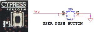
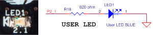
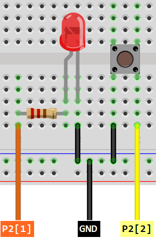
The CY8CKIT-059 board contains a single push button and a blue User LED. The push button connects the GND and the P2[2] pin and the blue user LED is connected to a resistor and P2[1] of the target PSoC 5LP device.
EagleSoC Development/Mini Board
Procedure
Creating a New Project
- Launch PSoC Creator.
- Got to File ➤ Open Project ➤ Project/Workspace.
- Open the PSoC5LP workspace in the EE4450 folder.
- After PSoC Creator opens the workspace, right-click on Workspace 'PSoC5LP' in the Workspace Explorer and select Add ➤ New Project...
- Select the correct PSoC5LP device model number, use the "Empty schematic" template, and enter the project name 02_GPIO_CCode.
Adding PSoC Creator Components
Follow the steps below to add components to the TopDesign.cysch in your PSoC Creator project:
- Add a Digital Input Pin:
- Open the component catalog under the Ports and Pins category.
- Drag and drop a
 Digital Input Pin onto the schematic.
- Add a Digital Output Pin:
- From the same Ports and Pins category, select Digital Output Pin.
- Drag and drop it onto the schematic.
- From the same Ports and Pins category, select
After completing these steps, you have successfully added both the Digital Input Pin and the Digital Output Pin to your schematic. You can now proceed with configuring the parameters and wiring them as required for the experiment:
Configure the Components
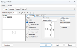
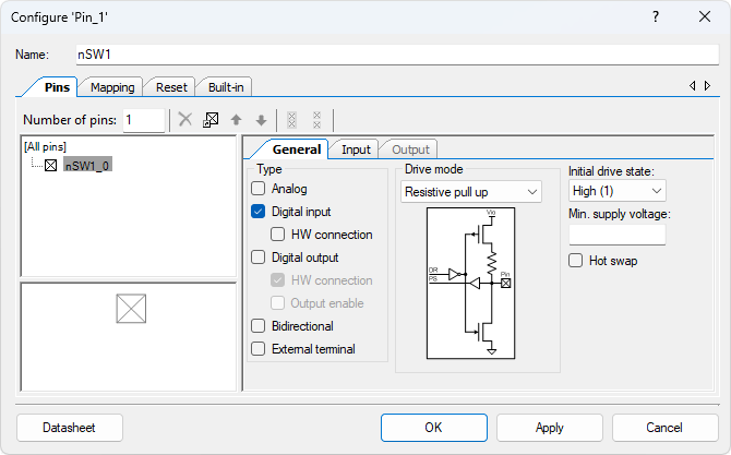
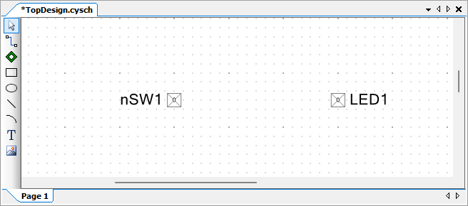
- Configure the Digital Input Pin (Pin_1):
- Click on the Pin_1 component in the schematic.
- Rename the component to nSW1 to reflect its function as a switch.
- Set the Drive Mode to Resistive pull-up, which ensures the pin defaults to high when not pressed.
- Uncheck the HW connection box to disable hardware connection, as shown in the diagram.
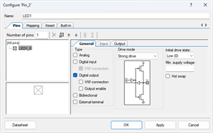
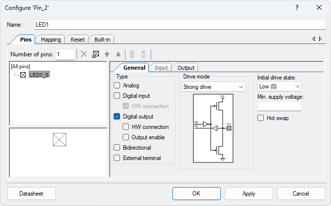
- Configure the Digital Output Pin (Pin_2):
- Select the Pin_2 component.
- Rename it to LED1 to indicate that it controls the LED.
- Uncheck the HW connection box, as the LED will be controlled by software.
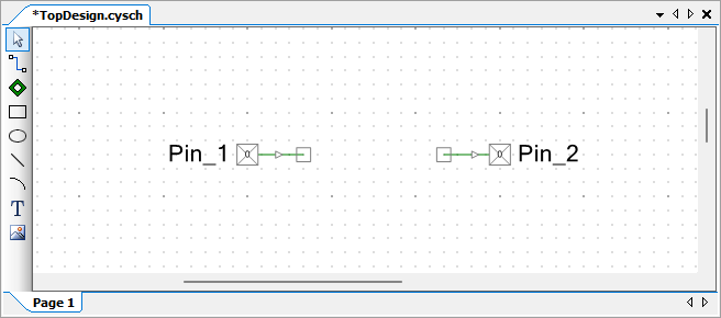
The new TopDesign.cysch file is shown below:
Click the Generate Application button to allow PSoC Creator to generate or update the various API files.
Pin Assignment
| Device | Port.Pin | Direction | Drive Mode |
|---|---|---|---|
Experiments
Experiment 1: LED Blinking with CyDelay()
Experiment 1: LED Blinking with CyDelay()
Make the on-board LED blink by turning it ON and OFF alternately with a 500-millisecond delay.
- Objective: Create a simple function to control the LED based on the switch's state.
- Steps:
- When the user presses the SW1 switch (connected to nSW1), the LED (connected to LED1) should turn on.
- When the user releases the switch, the LED should turn off.
- Implementation:
- In the C code, continuously check the state of nSW1. If the switch is pressed (input logic is low), set the LED1 pin high to turn on the LED. If the switch is released (input is high), set the LED1 pin low to turn it off.
Experiment 2: LED Control via SW1 Input
Experiment 2: LED Control via SW1 Input
Objective:
Control the LED based on the state of the SW1 button:
- When pressed (switch reads LOW), the LED is ON.
- When released (switch reads HIGH), the LED is OFF.
Concepts Introduced:
- Digital Input Pin reading.
- Direct mapping from input to output.
- Importance of input pin configuration with internal pull-up resistor.
- Basic use of if/else branching.
Key Notes:
- Mechanical switches often produce noise, resulting in rapid on/off signals (bouncing).
- In this simple experiment, no debounce delay is implemented yet.
- Switch is active LOW: pressed = 0, released = 1.
Experiment 3: LED Toggle with Falling-Edge Detection
Experiment 3: LED Toggle with Falling-Edge Detection
- Objective: Modify the function so that pressing the switch toggles the LED's state.
- Steps:
- When the user presses SW1 once, the LED should turn on.
- When the user presses SW1 again, the LED should turn off.
- Implementation:
- Implement a toggle mechanism using a flag. Each time the switch is pressed, check for a transition (from high to low), and alternate the state of LED1. This ensures the LED turns on and off with consecutive presses.